Inside the machine that saved Moore’s Law
The Dutch firm ASML spent $9 billion and 17 years developing a way to keep making denser computer chips.
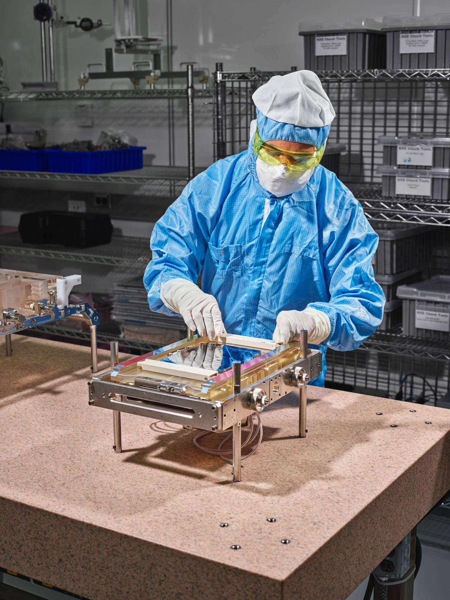
Patrick Whelan peers through the faceplate of his clean-room bunny suit to see how things are going.
Before him is a gleaming chunk of glass, roughly the size of a toaster oven, that is carved with so many scooped-out sections to reduce its weight that it looks like an alien totem. Whelan’s team is gluing it to a large, coffee-table-size piece of aluminum. Both metal and glass are eerily smooth, having been polished for weeks to remove minute imperfections. Over the next 24 hours, as the glue solidifies, workers will neurotically monitor the position of the glass and metal to make sure they fuse together just so.
“These will be placed together to microns of precision,” Whelan tells me, gesturing at the apparatus.
A nearby technician worries he’s too close, and yelps: Back up!
“I’m not touching! I’m not touching!” Whelan says, laughing.
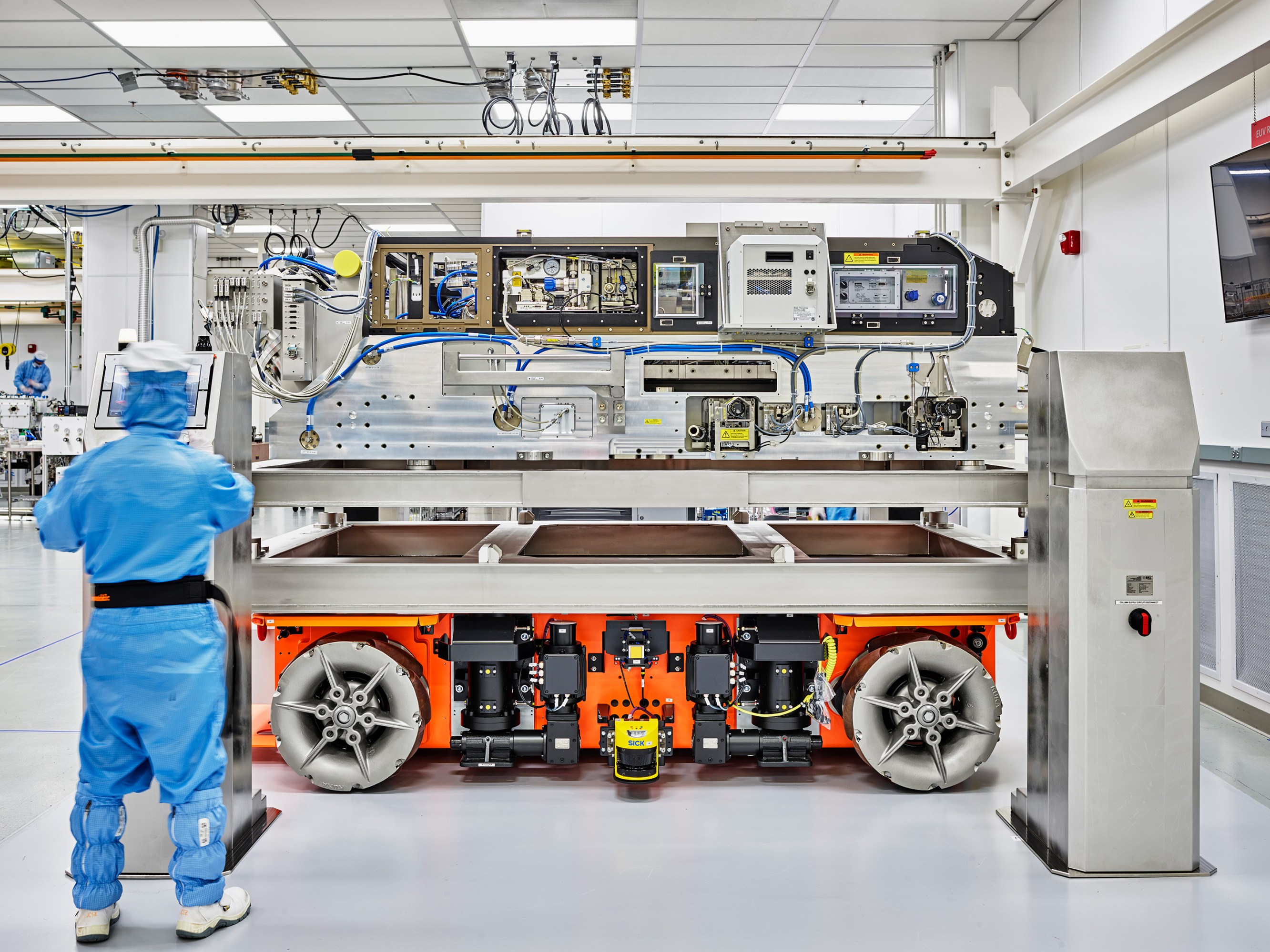
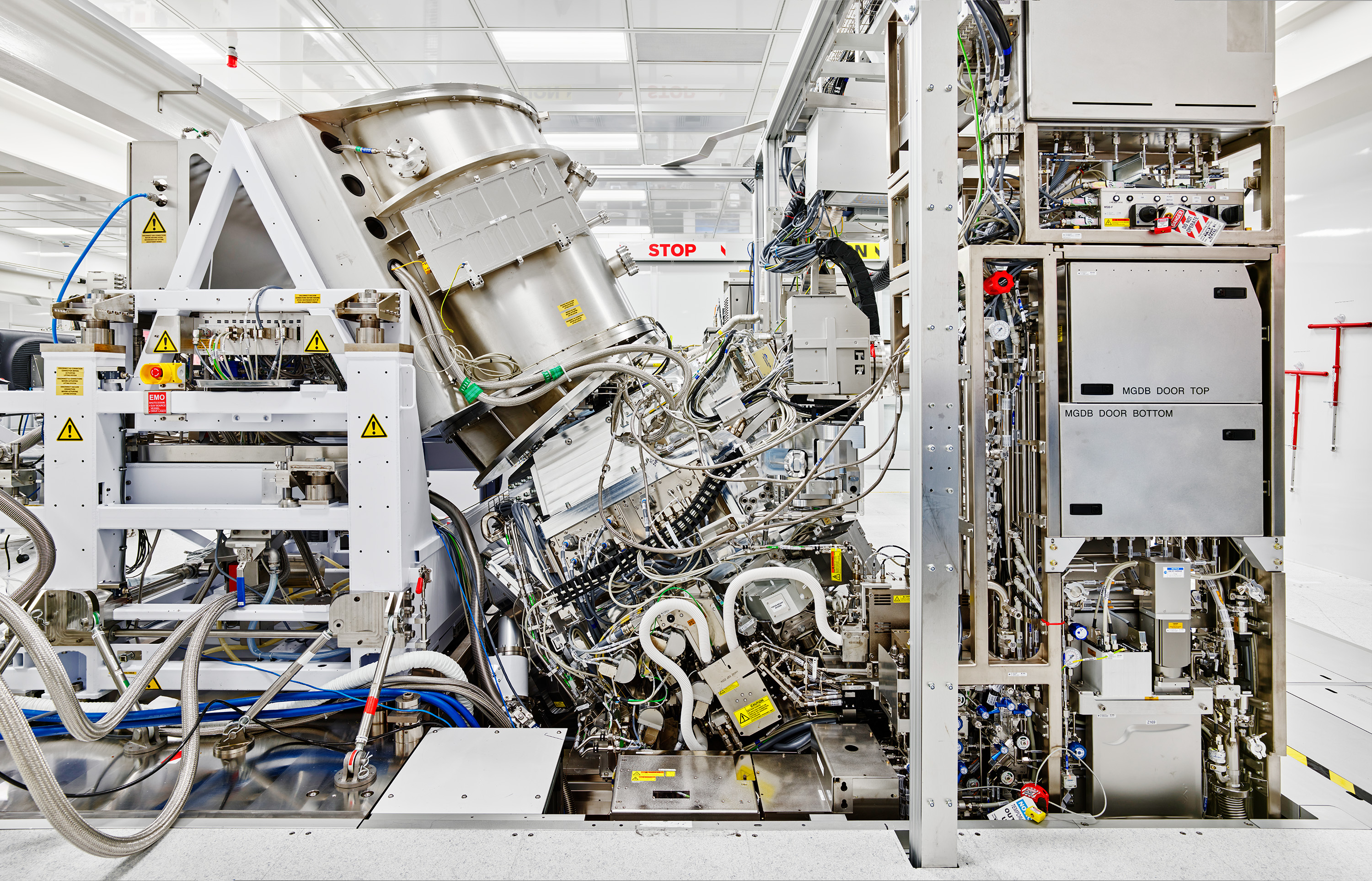
Precision is serious business here. I’m in Wilton, Connecticut, in a clean room of the Dutch company ASML, which makes the world’s most sophisticated machine for lithography—a crucial process used to create the transistors, wires, and other essential components of microchips. It’s a coveted device, with models costing as much as $180 million, that is used in making microchip features as tiny as 13 nanometers at a rapid clip. That level of precision is crucial if you’re Intel or TSMC and want to manufacture the world’s fastest cutting-edge computer processors. The final machine, assembled at ASML’s headquarters in the Netherlands, is the size of a small bus and filled with 100,000 tiny, coordinated mechanisms, including a system that generates a specific wavelength of high-energy ultraviolet light by blasting molten drops of tin with a laser 50,000 times a second. It takes four 747s to ship one to a customer.
“It’s a very difficult technology—in terms of complexity it’s probably in the Manhattan Project category,” says Sam Sivakumar, Intel’s director of lithography.
Here in Wilton, the glass-and-metal module that Whelan and his team are building is particularly critical. It will carry the patterns needed to make a microchip, and it’ll whiz back and forth while the machine blasts it with extreme ultraviolet (EUV) light, illuminating different parts of the chip pattern. The light will then bounce down to a dinner-plate-size wafer of silicon, burning the pattern in place.
Whelan walks over to a video monitor that shows one of these glass-metal contraptions zipping back and forth while being tested. It weighs 30 kilograms, but it moves in a blur.
“This is accelerating faster than a fighter jet,” Whelan says, his close-cropped beard and glasses obscured by his gear. “If there’s anything that’s loose, it’ll fly apart.” What’s more, he says, the apparatus has to stop on a spot the size of a nanometer—“so you have one of the fastest things on earth settling at pretty much the smallest spot of anything.”
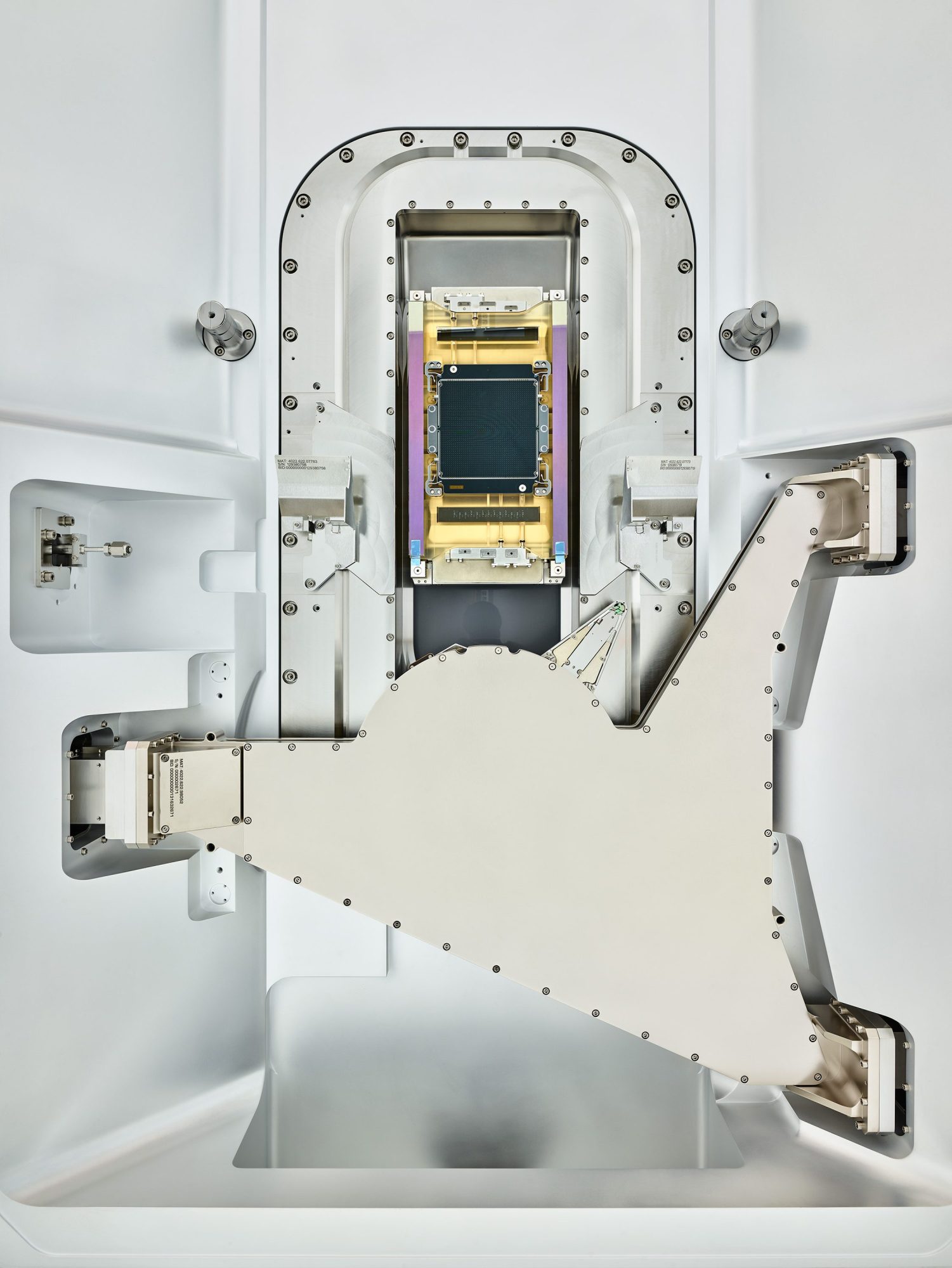
This combination of speed and accuracy is key to keeping up with Moore’s Law—the observation that the number of transistors crammed into a microchip doubles roughly every two years as components become ever smaller, making the chips cheaper and more powerful. The more tightly you pack transistors, the faster electrical signals can zip around the chip. Since the ’60s, chipmakers have shrunk the components by switching, every decade or so, to a new form of light with a smaller wavelength. But by the late ’90s, manufacturers were stuck at 193-nanometer light—and they were hotly debating what to do next. The situation grew more and more dire. Chipmakers had to use increasingly complex designs and techniques to keep Moore’s Law going, but they managed to eke out another two decades of increasing performance.
Then, in 2017, ASML unveiled its production-ready EUV machine, which uses light with a wavelength of just 13.5 nanometers. With a wavelength that short, chipmakers could pack transistors more densely than ever before. CPUs can crunch numbers faster, use less power, or just get smaller. The first generations of chips with tiny EUV features are already at work for huge firms like Google and Amazon, improving language translation, search-engine results, photo recognition, and even AI that, like GPT-3, talks and writes with an eerily human quality. The EUV revolution is also reaching everyday consumers, since ASML’s machines are being used to make chips for products including some Apple smartphones and Macs, AMD processors, and Samsung’s Note10+ phone. As EUV machines become more common, it’ll boost the performance and reduce the power demands on ever more everyday devices. EUV technology also enables simpler designs, which lets chipmakers move faster and produce more chips per wafer, resulting in cost savings that can be passed on to consumers.
The success of EUV lithography was far from guaranteed. The light is so devilishly hard to manipulate that for years experts predicted ASML would never figure it out. In fact, ASML’s rivals, Canon and Nikon, both gave up trying years ago. So ASML now has a corner on the market: if you want to create the most cutting-edge processors, you need one of its machines. ASML makes only 55 of them a year, and they sell briskly to the industry’s chip giants; currently over 100 are installed.
“Moore’s Law is basically falling apart, and without this machine, it’s gone,” says Wayne Lam, a director of research at CCS Insight. “You can’t really make any leading-edge processors without EUV.”
It’s extremely rare for a single firm to possess a monopoly on such a key part of microchip production. Even more astonishing is the sheer grind of work: it took ASML $9 billion of R&D and 17 years of research, a nonstop spree of experimentation, tweaking, and “aha” breakthroughs. EUV is now here—it’s working. But the effort and time it took to make it happen— and its late entry on the scene—raises some inevitable questions. How long will EUV be able to keep Moore’s Law going? And what will happen next?
When Jos Benschop joined ASML in 1997, he’d come off a long stint with Phillips and landed smack dab in a chip industry worried about its future. Over decades, engineers in chip fabrication had mastered the art of lithography. The concept is simple. You design the components of a chip—its wires and semiconductors—and then etch them into a series of “masks,” much as you make a stencil to put a pattern on a T-shirt. Then you put each mask over a silicon wafer and shine light through it (roughly equivalent to spraying paint over the stencil). The light hardens the “resist,” a chemical layer on the surface of the wafer; then other chemicals etch that pattern into the silicon. In the ’60s, chipmakers used visible light for this process, with a wavelength as small as 400 nanometers. Then they shifted to ultraviolet light, at 248 nm, and gradually reduced it to 193 nm—what’s often called deep UV. Each switch bought them several years’ extension of Moore’s Law.
But by the late ’90s, they’d focused deep UV as narrowly as they could manage, and they weren’t sure how to go smaller. It seemed that a new light source was needed. ASML at the time was a small firm of 300 people that had been successfully selling its deep-UV lithography tools. But to stay relevant, they realized, they’d need to do some serious R&D.
Benschop—a tall, angular executive with an exuberant but wry manner—was hired as the first research employee. He started going to big conferences, held twice a year, where deep thinkers from major chip firms and government agencies would stroke their chins and argue about what form of light to use next.
“What would be the next kid on the block?” was how Benschop put it when we spoke on Zoom this past summer. The experts pondered several options, all of which had huge problems. One idea was to use a spray of ions to draw patterns onto chips; that would work, but nobody could figure out how to do it rapidly at scale. The same went for shooting beams of electrons. Some advocated for using x-rays, which have a tiny wavelength, but they had challenges of their own. The final idea was extreme ultraviolet, with a wavelength that can go as low as 13.5 nanometers—pretty close to x-rays. It looked good.
The problem was that EUV would require an entirely new form of lithography machine. The existing ones used traditional glass lenses to focus light onto the wafer. But EUV light is absorbed by glass; it stops dead. If you wanted to focus it, you’d have to develop curved mirrors like the ones used in space telescopes. Worse, EUV is even absorbed by air, so you’d need to make the inside of your machine a perfectly sealed vacuum. And you’d need to generate EUV light reliably; nobody was sure how to do that.
Intel had tinkered with the idea, as had the US Department of Energy. But these were mostly lab experiments. To create a viable chipmaking lithography machine, you’d need to develop reliable techniques that could work quickly and produce chips in bulk.
After three years of pondering, in 2000 ASML decided to gamble the company and try to master EUV. They were a tiny firm, but if they could pull it off, they’d become a giant.
There were so many engineering problems to solve that, as Benschop recalls, “we didn’t have the momentum to do it ourselves.” So ASML’s executives began calling up the firms that had made components for their existing machines. One call went to Zeiss, the German optics firm that had for years made glass lenses for ASML.
Zeiss’s engineers had experience with EUV—including making extremely precise lenses and mirrors for x-ray telescopes. The trick was to coat the surface of the EUV mirrors with alternating layers of silicon and molybdenum, each only a few nanometers thick. Together they produce a pattern that reflects back as much as 70% of the EUV light that hits it.
The problem was in how to polish them. The machine would wind up needing 11 mirrors to bounce the EUV light around and focus it on the chip, rather like 11 Ping-Pong players bouncing a ball from one to another toward a target. Since the goal was to etch chip components measured in nanometers, each mirror had to be mind-bendingly smooth. The tiniest flaw would send EUV photons astray.
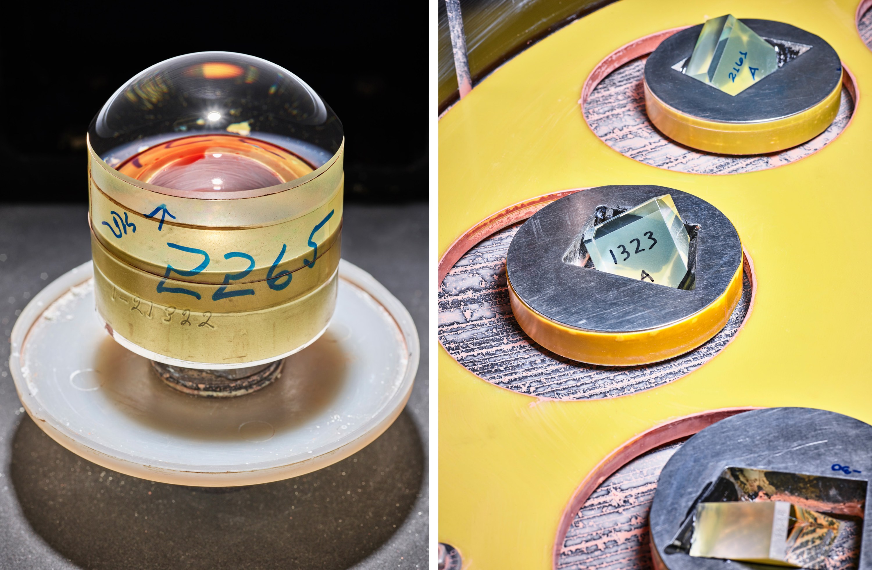
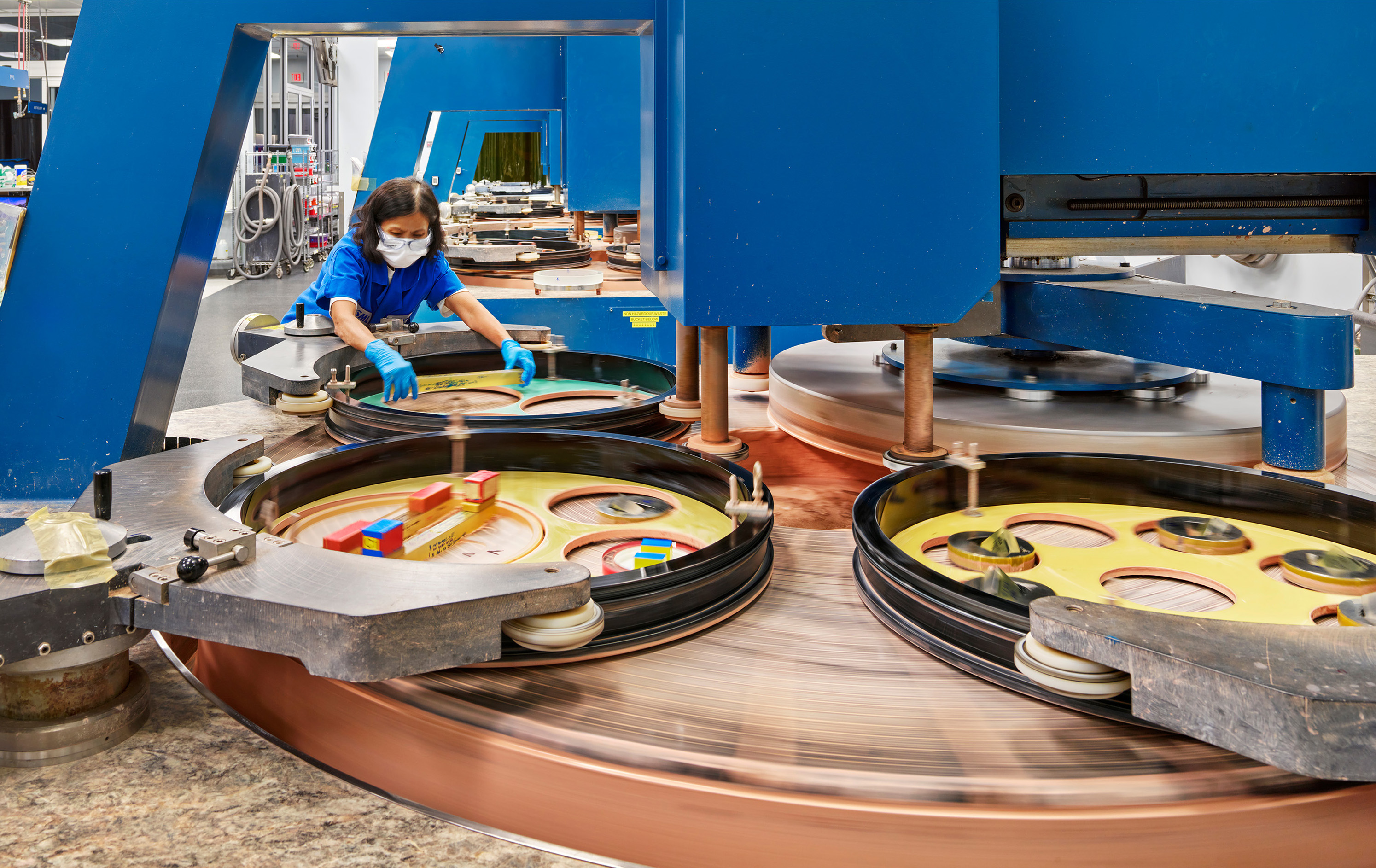
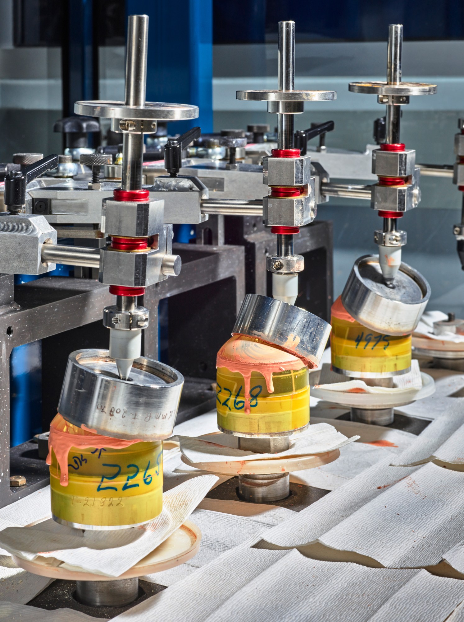
To give a sense of scale, if you took the mirror in your bathroom and blew it up to the size of Germany, it would have bumps about five meters high. Blown up to the same size, the smoothest EUV mirror Zeiss’s engineers had yet made—for space telescopes—would have bumps only two centimeters high. These mirrors for ASML would have to be orders of magnitude smoother: if they were the size of Germany, their biggest imperfections could be less than a millimeter high. “These are really the most precise mirrors in the world,” says Peter Kürz, who is responsible for the development of the next generation of EUV optics at Zeiss.
A big part of Zeiss’s work would be inspecting the mirrors to look for imperfections and then using an ion beam to knock individual molecules off, gradually smoothing the surface over months and months of work.
While Zeiss was developing the mirrors, Benschop and other ASML suppliers were working on their other big challenge: how to create a light source that would produce a steady flow of EUV.
It would haunt them for years.
To generate EUV, you need to create a plasma, a finicky phase of matter that exists only at extremely high temperatures. After early experiments zapping lithium with laser pulses to produce EUV light, they switched to tin, which produced bigger bursts.
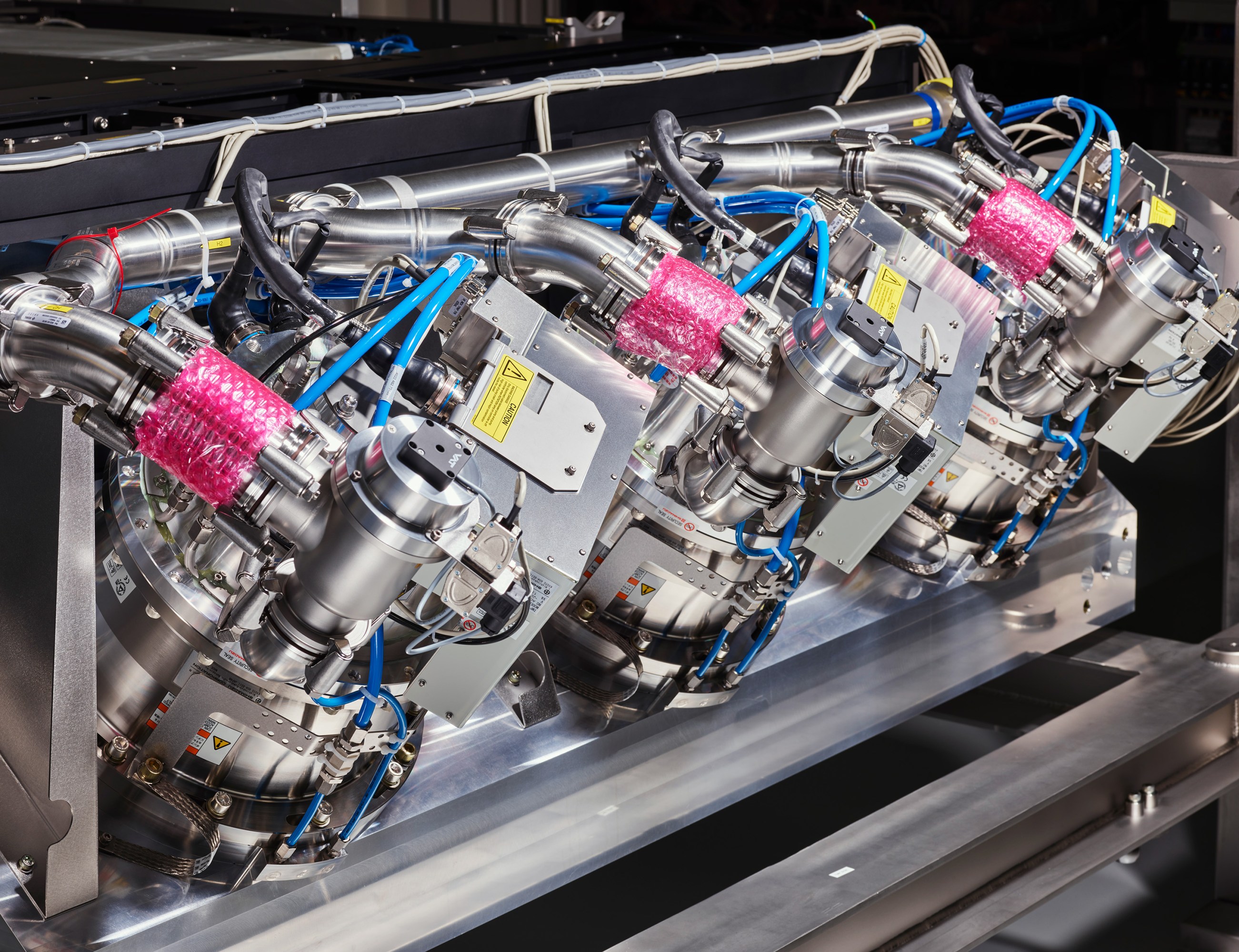
By the early 2000s, working with the San Diego firm Cymer and the German laser firm Trumpf, ASML had built something of a Rube Goldberg contraption. There’s a heated vessel that keeps tin in a liquid state. It feeds into a nozzle that shoots a droplet of molten tin—“a third of the diameter of a human hair,” says Danny Brown, the company’s Australian-born vice president of technical development—out into the bottom part of the machine, camera systems tracking its progress. When it reaches the center of the light-producing chamber, a laser pulse strikes the tin droplet. Immolated in a burst that reaches a temperature of about 500,000 K, the tin produces a plasma that glows with EUV light. The mechanism repeats this process, shooting and destroying tin droplets, 50,000 times a second.
“It’s non-straightforward, let’s put it that way,” Brown says drily.
Though they could now generate EUV light, Brown and his team quickly discovered new problems. Ions from the tin explosions would clog up the optics. To clean things up, they realized, they could pump hydrogen into the light chamber, where it would react with the tin ions and help scoop them away.
But they were rapidly falling behind schedule. Benschop had initially predicted that they’d have EUV machines “in volume” by 2006. In reality, by that year they had produced only two prototypes. The prototypes worked, etching patterns more finely than any lithography machine in history. But they were achingly slow. The light source was still too meager. In lithography, every photon matters; the more thickly you can generate them, the faster you can place a pattern down onto silicon.
Meanwhile, the machine was growing to unbelievably complex dimensions. It contained robot arms moving wafers, motors that accelerated the reticle—that big piece of glass that holds the pattern—to 32 times Earth’s gravity, and fully 100,000 parts, 3,000 cables, 40,000 bolts, and two kilometers of hosing. Worse, everything was interlinked: get one part working, and it’d create a problem somewhere else. It turned out, for example, that heat from the EUV light microscopically altered the dimensions of the mirrors. That forced Zeiss and ASML to develop sensors that would detect any change, triggering software that would shift the mirrors’ positions using precision actuators.
“As we corrected one problem, we moved on to the next,” Benschop says. “Every mountain you climbed, you saw the next mountain that was even higher.”
Many observers in the microchip industry, watching ASML fall behind schedule again and again, figured they’d fail.
“Ninety-five percent of the smart money thought that there was no way EUV would ever work,” says C.J. Muse, a semiconductor industry analyst with Evercore.
While ASML beavered away at EUV, they and the rest of the industry were performing ever more elaborate tricks to extend the performance of deep UV light as much as possible, to pack more transistors onto chips. One technique, called “immersion,” involved putting a layer of water over the chip, which refracted incoming light and allowed it to be focused in a tighter pattern.
Lithography engineers also developed a technique for patterning and carving away at a chip layer multiple times—what’s known as “multiple patterning”—to produce finer details. Together, these approaches pushed chip components down to 20 nanometers.
But these oddball innovations also made the act of chipmaking much more complex. Immersion required managing the presence of water in the delicate lithography process, no easy task. And chip designers found it onerous to change their designs to work with multiple patterning. Deep UV was running out of steam—and everyone knew it.
By the mid-2010s, though, it began to seem as if EUV might finally come to the rescue. Brown and his team had dived into the scientific literature, looking for ways to get more out of each tin droplet. As a former university researcher who studied plasma physics, he was known inside ASML for raising pointy-headed scientific issues; the CTO jokingly gave him a plaque emblazoned with the words “Scientifically Accurate But Practically Useless.”
This time, though, soaking in the scientific literature paid off. It suggested the concept of hitting each tin droplet with the laser twice. A first blast would flatten the droplet into a pancake shape, which enabled a second blast—millionths of a second later—to produce far more EUV. Brown’s team devised a way to do this at scale.
Other discoveries came by happy accident. As their ability to immolate tin improved, the process produced more debris than the hydrogen could clean up. Mirror performance was degrading. Then one day they noticed something funny: the mirrors didn’t degrade as quickly after the machine had been opened for maintenance. As it turned out, oxygen in the air that came in helped reverse the contamination. ASML built the occasional addition of small amounts of oxygen into the design.
By the middle of 2017, the company finally had a working demo that etched chips at an industry-friendly pace—125 wafers per hour. From his office in San Diego, Brown watched the demo in the Netherlands. He was elated; he’d changed into a Hawaiian shirt, proclaiming that he’d finally be able to go on vacation.
“This thing was like zzzt zzzt zzzt zzzt,” he recalls, mimicking the speed of the reticle zipping around, and the robotic arm sliding in a new wafer about every 30 seconds. “It was the last domino to basically say, ‘Yeah, EUV lithography will happen.’”
That year, ASML began finally shipping out machines that would revolutionize chipmaking. Once the market realized that ASML had a monopoly on the cutting-edge tools, its stock began to soar, reaching $549 and making the company’s market cap almost the size of Intel’s.
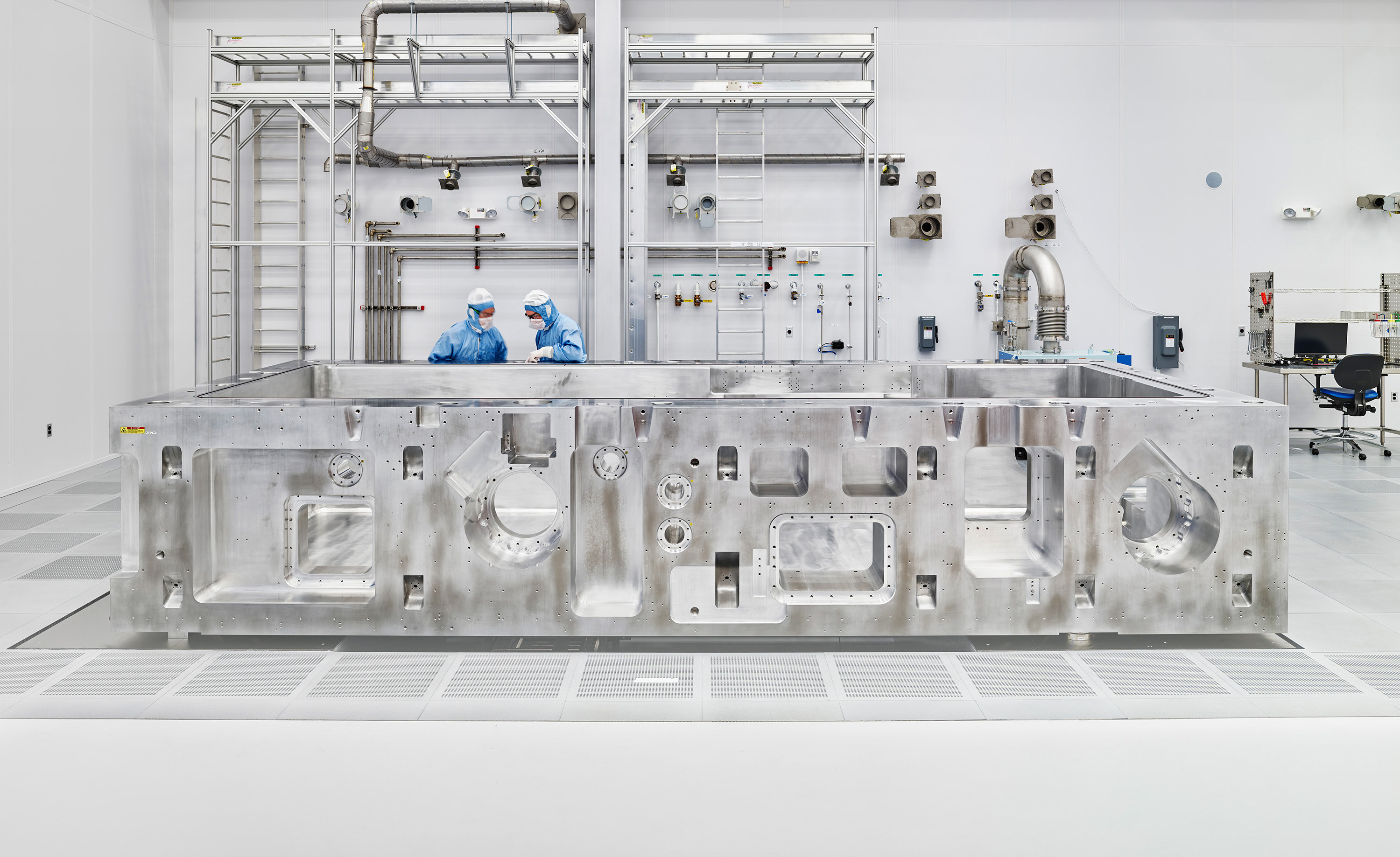
If you’re a gearhead like me, the machine is truly gorgeous to behold—a marvel of engineering. When I visited Wilton, they walked me over to view a massive block of milled aluminum that forms the top part of the device. It is eight feet long, six feet wide, and two feet thick. Gleaming like the chassis of a spaceship, it holds the glass reticle and also has mounted on it huge, barrel-shaped molecular pumps. Each pump contains tiny blades that spin at 30,000 RPM, sucking all gases out of the machine to produce a vacuum within. “They actually smack the molecules of the gas out of the way, one at a time,” Whelan told me.
One could argue that ASML’s chief success has not been so much in making machinery as in measuring it. When I pulled off my bunny suit, I visited the machine shop, where huge chunks of glass were being carved for the reticle. After each piece of glass is milled, it’s placed on machines that gradually smooth it for hundreds of hours over several weeks. As machine-shop manager Guido Capolino told me, they measure the glass all along to see how many imperfections are being removed, starting with coarse microns. He gestured at a polishing machine behind us, where glass pieces slowly revolved on top a slurry of wet polishing mix.
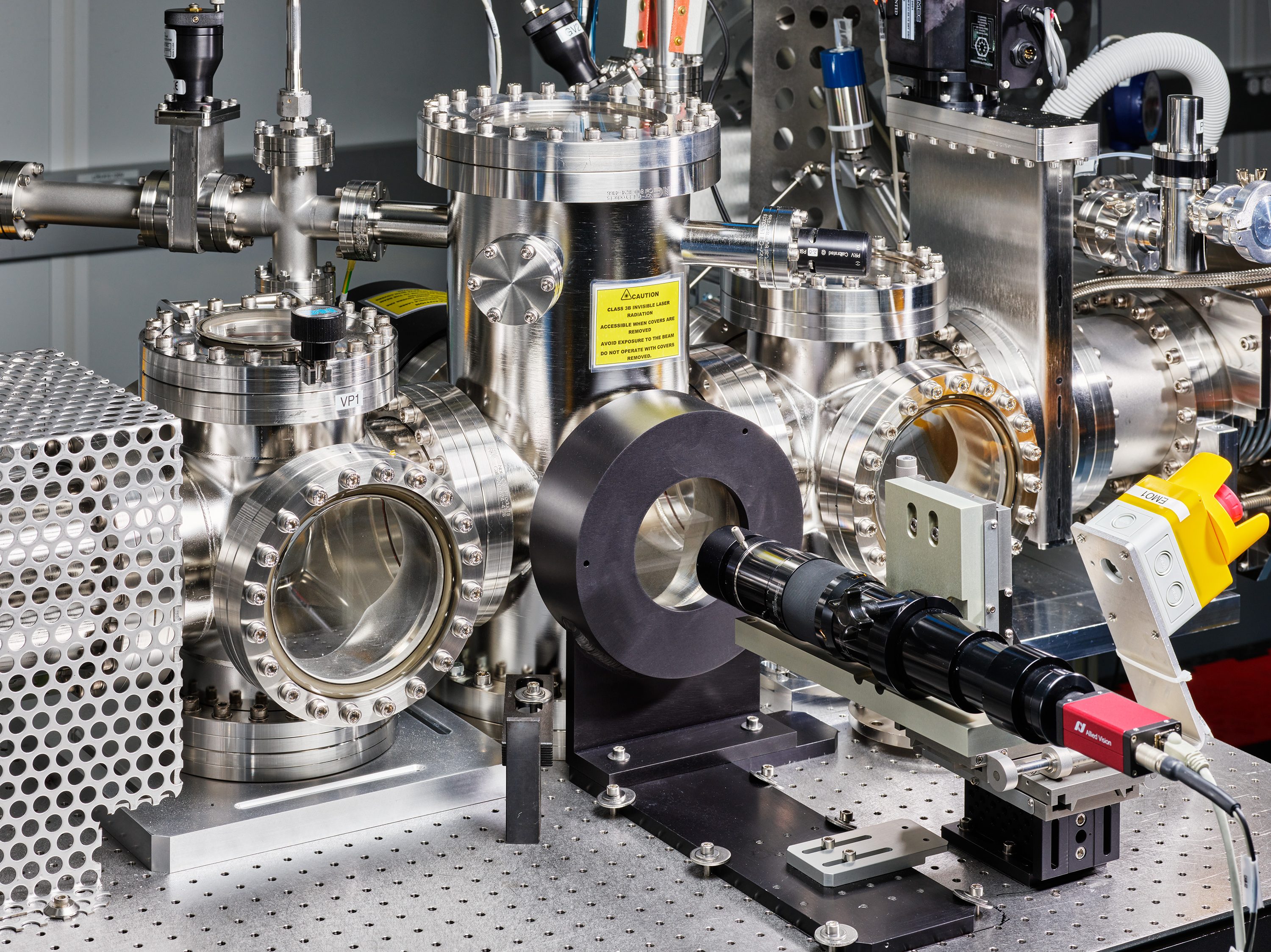
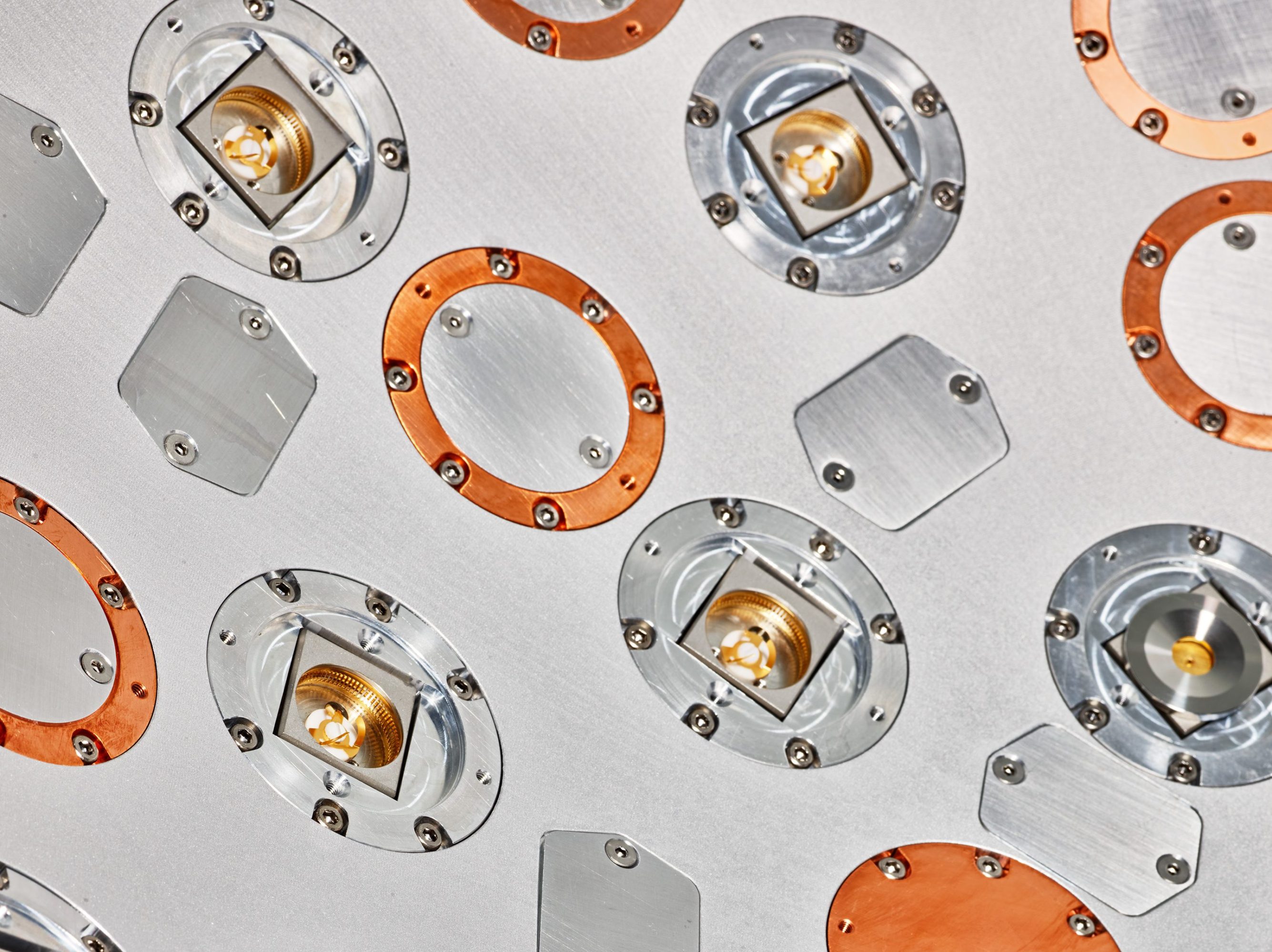
“We’re down at angstroms and nanometers for the variability here,” he said. Using glass in the reticle is crucial; it doesn’t deform under heat as much as metal. But it’s devilishly hard to carve—yet another problem the engineers had to slowly solve.
ASML’s success with EUV has won the company deep respect across the microchip industry. Chris Mack, a four-decade veteran of chip lithography, is currently the chief technology officer for Fractilia, a firm that makes software for chipmaking. He says the reason ASML and its partners succeeded—where others never even dared to try—is sheer, dogged persistence.
“They peeled the onion,” he told me. “They go, Oh, now I got the next layer. And then they pull that layer. And then nobody really knows whether it’s rotten in the core or it’s going to be good. They just keep peeling it. And to their credit, they just never gave up.”
Now that they have the ability to keep crafting smaller and smaller components, major firms like Intel and TSMC and Samsung can build ever faster and more power-conserving chips.
“Our designers can breathe a sigh of relief,” says Intel’s Sam Sivakumar. “Moore’s Law is alive.”
As more EUV machines come online and their cost amortizes, the technology will trickle down to an increasing number of everyday devices. The one place that won’t benefit from the EUV revolution—at least in the short term—is China.
Worried that China poses a technological threat, both the Trump and Biden administrations successfully pressured the Netherlands to prevent ASML from selling EUV machines to customers there.
Can China simply make its own EUV devices? Some industry observers suspect it can’t. ASML’s success with EUV required enormous collaboration with firms based everywhere from Germany and the US to Japan (which makes chemicals critical to the lithographic masks). China, being relatively isolated, stands little chance on its own, according to Will Hunt, an analyst with Georgetown University’s Center for Security and Emerging Technology. “It can’t really close that gap,” he says.
What’s possible, other observers suggest, is that there’ll simply be a delay in China’s ability to buy EUV machines. Typically, China’s chipmakers work with last-generation tools that are a step behind what’s used by TSMC in Taiwan, Samsung in Korea, or Intel in the US, C.J. Muse says. So when ASML’s first generation of EUV machines become a bit older—a few years from now—and the industry moves on to newer models, China might be allowed to buy them.
And in fact, ASML is already working on an improved version of the device. It will be able to focus EUV light to an even sharper degree thanks to what’s known as a higher numerical aperture, allowing it to etch components that could be under 10 nanometers wide. This “high-NA” EUV machine will have larger mirrors, requiring the entire machine to get larger too. Intel is currently the first customer for one of these next-generation machines, and it expects to sell its first chips built with them by 2025.
ASML and most observers figure EUV will help chips progress until at least 2030, and possibly longer. After all, some of the tricks that chip designers developed to keep deep UV going for so long should be repeatable with EUV.
But at some point in the next decade or so, the chip industry’s desire to shrink features will start bumping up against some physical limitations that are even harder than the ones they’ve currently bested. For one thing, quantum problems begin to emerge. Indeed, they already have: chipmakers using ASML’s EUV machines have to wrestle with “stochastic errors”—rays of EUV light naturally go astray, producing incorrect patterns on chips. These aren’t show-stopping problems yet, but they’ll furrow brows more and more the smaller chipmakers go.
Assuming “high NA” keeps Moore’s Law going to 2030, what will take over then? Industry experts figure ASML will continue to explore even higher-numerical-aperture devices, allowing them to focus EUV on smaller and smaller points. At the same time, chip designers are looking into strategies for improving chips that aren’t so dependent on further miniaturization, such as extending architectures upward and building into the third dimension by stacking chip layers. As to what lithography technology might come after EUV, no one yet knows. Intel’s Sivakumar wouldn’t speculate; Mack said that outside of high-NA EUV, “nothing else” is under intensive development.
Inside the Wilton clean room, Whelan gave me a peek at their high-NA EUV machine. He rolled up a huge garage-style door and ushered me into a massive new clean room the size of a football field. In the corner was a shiny aluminum reticle bed. It was just like the one I’d seen for the original EUV machine, but it could no longer fit comfortably in a living room; it was almost as big as a subway car and weighed fully 17 tons. They had to install cranes in the roof to move it.
“So this,” Whelan said, “is going to be the machine that helps us continue pushing Moore’s Law into the future.”
Correction: An earlier version of this article stated that more than 1,000 EUV machines have been installed. In actuality, it is more than 100.
Clive Thompson is a science and technology journalist based in New York City and author of Coders: The Making of a New Tribe and the Remaking of the World.
Deep Dive
Computing
Inside the hunt for new physics at the world’s largest particle collider
The Large Hadron Collider hasn’t seen any new particles since the discovery of the Higgs boson in 2012. Here’s what researchers are trying to do about it.
How ASML took over the chipmaking chessboard
MIT Technology Review sat down with outgoing CTO Martin van den Brink to talk about the company’s rise to dominance and the life and death of Moore’s Law.
How Wi-Fi sensing became usable tech
After a decade of obscurity, the technology is being used to track people’s movements.
Algorithms are everywhere
Three new books warn against turning into the person the algorithm thinks you are.
Stay connected
Get the latest updates from
MIT Technology Review
Discover special offers, top stories, upcoming events, and more.